| CPC H01L 23/481 (2013.01) [H01L 27/0207 (2013.01); H01L 27/088 (2013.01)] | 9 Claims |
|
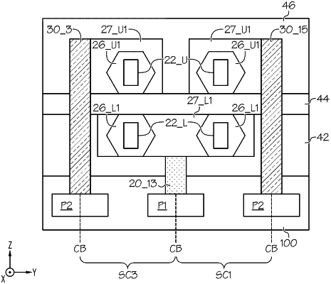
1. An integrated circuit device comprising:
a plurality of standard cells arranged on a substrate in multiple rows that each extend in a first direction, wherein the plurality of standard cells comprises a first standard cell in a first row and a second standard cell in a second row that is immediately adjacent to the first row,
wherein each of the first and second standard cells comprises:
an upper transistor comprising:
an upper active region;
an upper gate structure on the upper active region; and
an upper source/drain region on the upper active region;
a lower transistor between the substrate and the upper transistor, the lower transistor comprising:
a lower active region;
a lower gate structure on the lower active region; and
a lower source/drain region on the lower active region;
a first power line and a second power line;
a first power via electrically connecting the first power line to the lower source/drain region; and
a second power via electrically connecting the second power line to the upper source/drain region, and
wherein the first power via of the first standard cell and the first power via of the second standard cell are aligned with each other along the first direction.
|