| CPC H01L 23/481 (2013.01) [H01L 24/17 (2013.01); H01L 24/33 (2013.01)] | 6 Claims |
|
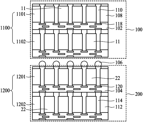
1. A method for manufacturing a semiconductor device, comprising:
preparing a first group of wafers having a plurality of first semiconductor dies embedded in a first photosensitive material layer;
forming a plurality of first through vias in the first photosensitive material layer;
attaching at least two of the first group of wafers using a first adhesive layer to form a first structure;
forming a first redistribution layer formed within the first adhesive layer, wherein the plurality of first through vias are connected to the first redistribution layer;
preparing a second group of wafers having a plurality of second semiconductor dies embedded in a second photosensitive material layer;
forming a plurality of second through vias in the second photosensitive material layer;
attaching at least two of the second group of wafers using a second adhesive layer to form a second structure;
forming a second redistribution layer formed within the second adhesive layer, wherein the plurality of second through vias are connected to the second redistribution layer; and
connecting the first structure to the second structure with a plurality of first metal bumps.
|