| CPC H01L 23/295 (2013.01) [H01L 21/561 (2013.01); H01L 21/565 (2013.01); H01L 23/291 (2013.01); H01L 23/3114 (2013.01); H01L 23/3128 (2013.01); H01L 23/5283 (2013.01); H01L 24/09 (2013.01); H01L 24/17 (2013.01); H01L 24/97 (2013.01)] | 15 Claims |
|
1. A method of manufacturing a semiconductor package, the method comprising:
mounting at least one semiconductor chip on top of a package substrate;
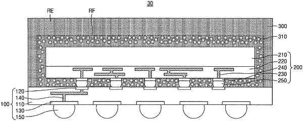
coating a molding material including fillers including an electromagnetic material on the package substrate to surround the at least one semiconductor chip,
moving the fillers in a certain direction in the molding material by applying an electric field or a magnetic field to the molding material; and
forming a molding member to surround the at least one semiconductor chip by curing the molding material, wherein
the molding member covers a bottom surface, a side surface, and top surfaces of the at least one semiconductor chip, wherein
the mounting the semiconductor chip includes mounting the semiconductor chip on the package substrate using solder bumps and the moving the fillers includes applying an electric field or a magnetic field such that the fillers are moved to be placed around each of the solder bumps and placed in a relatively high distribution in a region between the semiconductor chip and the package substrate in the molding material, or
the moving the fillers includes applying an electric field or a magnetic field such that the fillers are spaced apart from the semiconductor chip and placed in a relatively high distribution in the molding material at a peripheral region of the semiconductor chip, or
the moving the fillers includes applying an electric field or a magnetic field such that the fillers are spaced apart from the semiconductor chip and placed in a relatively high distribution in an upper region of the molding material.
|