| CPC H01L 21/823857 (2013.01) [H01L 21/823821 (2013.01); H01L 27/0924 (2013.01); H01L 21/0228 (2013.01); H01L 21/02178 (2013.01); H01L 21/02192 (2013.01); H01L 21/28185 (2013.01); H01L 21/3115 (2013.01); H01L 21/31111 (2013.01)] | 20 Claims |

|
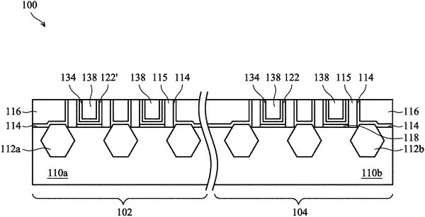
1. A semiconductor device comprising:
a first transistor having a first active region, the first transistor comprising a first gate structure, the first gate structure comprising:
a first high-k dielectric layer over a portion of the first active region, the first high-k dielectric layer being substantially free of lanthanum; and
a first gate electrode over the first high-k dielectric layer; and
a second transistor having a second active region, the second transistor comprising a second gate structure, the second gate structure comprising:
a second high-k dielectric layer over a portion of the second active region, the second high-k dielectric layer comprising lanthanum, wherein a ratio of lanthanum to titanium in the second high-k dielectric layer is greater than about 50; and
a second gate electrode over the second high-k dielectric layer.
|