| CPC H01L 21/762 (2013.01) [H01L 21/02164 (2013.01); H01L 21/02181 (2013.01); H01L 21/02225 (2013.01); H01L 21/2253 (2013.01); H01L 21/76229 (2013.01); H01L 21/76232 (2013.01); H01L 29/165 (2013.01); H01L 29/42316 (2013.01); H01L 29/66545 (2013.01); H01L 29/66553 (2013.01); H01L 29/785 (2013.01); H01L 29/7848 (2013.01)] | 20 Claims |
|
1. A method of forming an integrated circuit device, the method comprising:
sequentially forming a first epitaxial layer and a second epitaxial layer on a substrate, wherein the first epitaxial layer comprises a material different from the second epitaxial layer, and a thickness of the first epitaxial layer is from about 10 Å to about 100 Å;
implanting dopants into the second epitaxial layer to form a preliminary impurity region in the second epitaxial layer;
heating the substrate to convert the preliminary impurity region into an impurity region;
forming a third epitaxial layer on the substrate after heating the substrate;
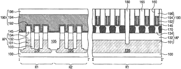
forming a first trench and a second trench in the third epitaxial layer and the impurity region to define an active in between the first trench and the second trench;
forming a first isolation layer and a second isolation layer in the first trench and the second trench, respectively, wherein the active fin protrudes beyond upper surfaces of the first and second isolation layers such that the first and second isolation layers expose opposing sides of the active fin;
forming a gate insulation layer extending on the opposing sides and an upper surface of the active fin; and
forming a gate electrode traversing the active fin.
|