| CPC H01L 21/67288 (2013.01) [G01N 23/203 (2013.01); G01N 23/2251 (2013.01); H01J 37/244 (2013.01); H01J 37/26 (2013.01); G01N 2223/6116 (2013.01); G01N 2223/646 (2013.01)] | 20 Claims |
|
1. A solid state device, the device comprising:
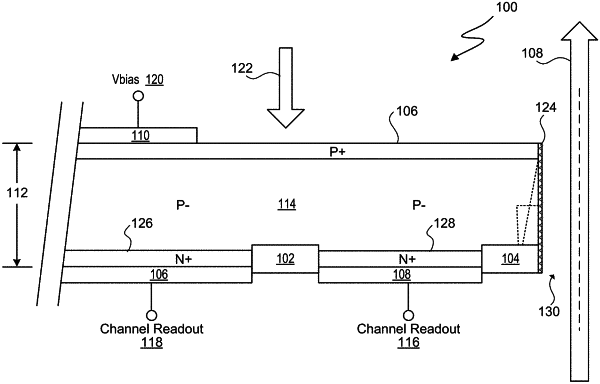
a vertical structure comprising an N+/P−/P+ or a P+/N−/N+ structure for full depletion through the thickness of the device, the N+/P−/P+ or a P+/N−/N+structure including an N+ or P+ junction formed on the front side of the device, a P− or N− intrinsic layer in the middle, and a P+ or N+ layer formed on the backside of the device;
an active area for collecting secondary electrons (SEs) and backscatter electrons (BSEs), the active area being segmented into multiple channels in order to separate detection of secondary and backscatter electrons; and
a through hole placed in the center of the device to allow a primary beam to pass through the device, wherein the primary beam enters the through hole on the front side of the device.
|