| CPC H01G 4/30 (2013.01) [H01G 4/012 (2013.01); H01G 4/1227 (2013.01); H01G 4/248 (2013.01)] | 20 Claims |
|
1. A multilayer ceramic electronic component, comprising:
a ceramic body including a dielectric layer and a plurality of internal electrodes disposed to oppose each other with the dielectric layer interposed therebetween, and having a first surface and a second surface opposing each other in a thickness direction of the ceramic body, a third surface and a fourth surface connected to the first surface and the second surface, and opposing each other in a length direction of the ceramic body, and a fifth surface and a sixth surface connected to the first surface to the fourth surface, and opposing each other in a width direction of the ceramic body; and
an external electrode disposed outside the ceramic body, and electrically connected to one or more of the plurality of internal electrodes,
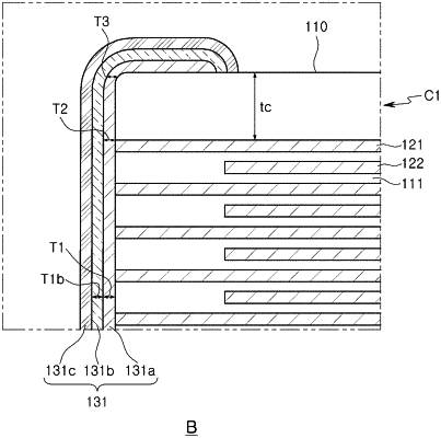
wherein the external electrode includes an electrode layer electrically connected to the one or more of the plurality of internal electrodes, a first plating layer disposed on the electrode layer, and a second plating layer disposed on the first plating layer,
a thickness T1 of the electrode layer corresponding to a central region of the ceramic body in the thickness direction is 5 μm or more and 30 μm or less, a thickness T2 of the electrode layer corresponding to a region in which an outermost internal electrode, of the internal electrodes, is located is 5 μm or more and 15 μm or less, and a thickness T3 of the electrode layer corresponding to a corner portion of the ceramic body is more than 0.1 μm and less than 10 μm, in a cross-section of the ceramic body in the thickness and length directions, and
a thickness of the dielectric layer is 0.4 μm or less, and a thickness of one of the plurality of the internal electrodes is 0.4 μm or less.
|