| CPC G11C 29/54 (2013.01) [G01R 31/3181 (2013.01); G11C 7/065 (2013.01); G11C 7/067 (2013.01); G11C 29/16 (2013.01); H10B 80/00 (2023.02); G01R 31/3177 (2013.01); H01L 25/065 (2013.01); H01L 25/0652 (2013.01); H01L 25/0655 (2013.01); H01L 25/0657 (2013.01); H01L 25/18 (2013.01)] | 20 Claims |
|
1. An apparatus, comprising:
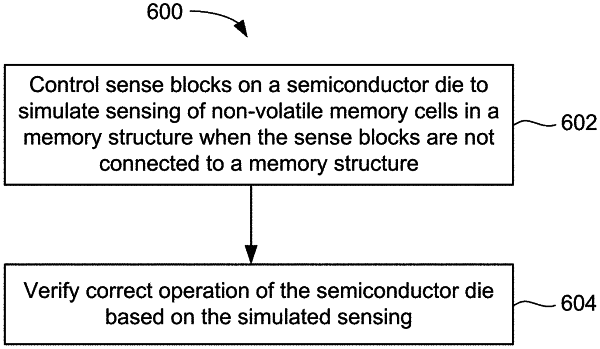
a semiconductor die comprising a plurality of sense blocks and a control circuit in communication with the plurality of sense blocks, the sense blocks configured to be connected to a memory structure having non-volatile memory cells, wherein the control circuit is configured to:
control the plurality of sense blocks to simulate sensing of non-volatile memory cells in the memory structure when the sense blocks are not connected to the memory structure; and
verify correct operation of the semiconductor die based on the simulated sensing.
|