| CPC G11C 29/44 (2013.01) [G11C 29/18 (2013.01); G11C 29/36 (2013.01); G11C 29/46 (2013.01)] | 9 Claims |
|
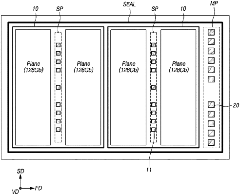
1. A layout of a semiconductor memory device comprising:
a plurality of chip regions each including a plurality of planes arranged in a first direction;
a main pad region extending in a second direction perpendicular to the first direction and including a plurality of main pads arranged in the second direction;
a plurality of sub pad regions, each extending in the second direction and including a plurality of sub pads arranged in the second direction;
wherein each of the plurality of planes corresponds to one of the plurality of main pads;
wherein each of the plurality of planes is directly connected to at least one of the plurality of sub pads, which is connected to the corresponding one of the main pads through a redistribution line; and
wherein a width of the main pad region in the first direction is greater than a width of the sub pad region in the first direction.
|