| CPC G11C 19/184 (2013.01) [G09G 3/3648 (2013.01); G09G 3/3677 (2013.01); G09G 3/3266 (2013.01); G09G 2300/0426 (2013.01); G09G 2310/0267 (2013.01); G09G 2310/0275 (2013.01); G09G 2310/0286 (2013.01); G09G 2310/0289 (2013.01); G09G 2320/02 (2013.01); G09G 2320/043 (2013.01); G09G 2330/021 (2013.01); G09G 2330/023 (2013.01)] | 5 Claims |
|
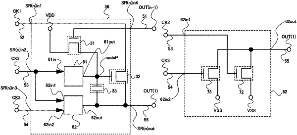
1. A semiconductor device comprising:
a first transistor;
a second transistor;
a third transistor; and
a fourth transistor,
wherein one of a source and a drain of the first transistor, one of a source and a drain of the second transistor, and an output terminal are electrically connected to one another,
wherein a gate of the first transistor, one of a source and a drain of the third transistor, and one of a source and a drain of the fourth transistor are electrically connected to one another,
wherein a gate of the second transistor and a gate of the third transistor are electrically connected to one another,
wherein a gate signal line is electrically connected to the output terminal,
wherein a power source line is electrically connected to the other of the source and the drain of the second transistor, and the other of the source and the drain of the third transistor,
wherein a clock signal line is electrically connected to the other of the source and the drain of the first transistor, and
wherein, in a top view, a first conductive layer, a second conductive layer, and a third conductive layer are arranged so that the first conductive layer functioning as the power source line is located between the second conductive layer functioning as the clock signal line and the third conductive layer functioning as the output terminal, and the second conductive layer functioning as the clock signal line is not located between the first conductive layer functioning as the power source line and the third conductive layer functioning as the output terminal.
|