US 11,699,488 B2
Device-region layout for embedded flash
Shih Kuang Yang, Tainan (TW); Ping-Cheng Li, Kaohsiung (TW); Hung-Ling Shih, Tainan (TW); Po-Wei Liu, Tainan (TW); Wen-Tuo Huang, Tainan (TW); Yu-Ling Hsu, Tainan (TW); Yong-Shiuan Tsair, Tainan (TW); and Chia-Sheng Lin, Tainan (TW)
Assigned to Taiwan Semiconductor Manufacturing Company, Ltd., Hsinchu (TW)
Filed by Taiwan Semiconductor Manufacturing Company, Ltd., Hsin-Chu (TW)
Filed on Oct. 21, 2021, as Appl. No. 17/506,904.
Application 16/952,411 is a division of application No. 16/400,361, filed on May 1, 2019, granted, now 10,861,553, issued on Dec. 8, 2020.
Application 17/506,904 is a continuation of application No. 16/952,411, filed on Nov. 19, 2020, granted, now 11,158,377.
Claims priority of provisional application 62/737,288, filed on Sep. 27, 2018.
Prior Publication US 2022/0044729 A1, Feb. 10, 2022
This patent is subject to a terminal disclaimer.
Int. Cl. G11C 16/08 (2006.01); G11C 11/16 (2006.01); H10B 12/00 (2023.01); H10B 41/30 (2023.01)
CPC G11C 16/08 (2013.01) [G11C 11/1657 (2013.01); H10B 12/053 (2023.02); H10B 41/30 (2023.02)] 20 Claims
OG exemplary drawing
 
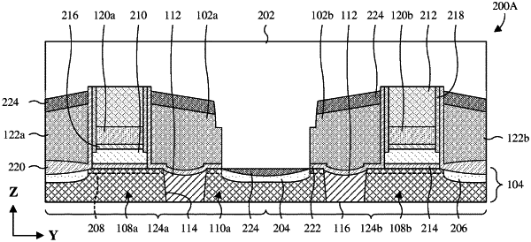
1. An integrated chip comprising:
a substrate;
a first source/drain region and a second source/drain region in the substrate;
an erase gate, a control gate, and a word line overlying the substrate, wherein the erase gate overlies the first source/drain region, wherein the word line borders the second source/drain region, and wherein the control gate is between and borders the erase gate and the word line; and
a trench isolation structure extending into the substrate, wherein the trench isolation structure is between the first and second source/drain regions, and is closer to the second source/drain region than the first source/drain region, along an axis.