| CPC G11C 16/08 (2013.01) [G11C 16/0483 (2013.01); G11C 16/24 (2013.01); G11C 16/26 (2013.01)] | 12 Claims |
|
1. A semiconductor memory device comprising:
a cell string including at least one drain select transistor that is connected to a bit line, at least one source select transistor that is connected to a common source line, and a plurality of memory cells that are connected between the drain select transistor and the source select transistor; and
a peripheral circuit configured to perform a read operation on a selected memory cell among the plurality of memory cells,
wherein the peripheral circuit is configured to:
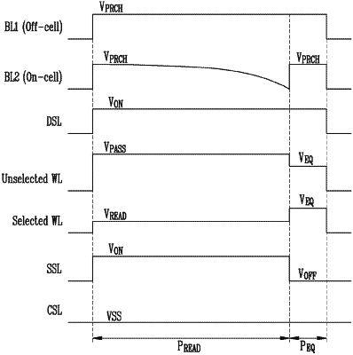
read data that is stored in the selected memory cell by applying a read voltage to a selected word line among word lines that are connected to the plurality of memory cells and by applying a pass voltage to unselected word lines
apply a turn-on voltage to a drain select line that is connected to the drain select transistor;
apply a turn-off voltage to a source select line that is connected to the source select transistor while applying the turn-on voltage to the drain select line; and
apply a boosting prevention voltage to the bit line while applying an equalizing voltage to the word lines.
|