| CPC G11C 11/4094 (2013.01) [G11C 11/4085 (2013.01); G11C 11/4091 (2013.01); H10B 12/30 (2023.02); H10B 12/50 (2023.02); G11C 7/12 (2013.01)] | 18 Claims |
|
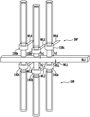
1. A memory device, comprising:
a first bit line and a second bit line which are arranged in parallel on a first plane;
a lower word line arranged to intersect the first and the second bit lines to form lower memory cells, the lower word line arranged in a second plane located below the first plane on which the first and second bit lines are arranged; and
an upper word line arranged to intersect the first and the second bit lines to form upper memory cells, the upper word line arranged in a third plane located above the first plane,
wherein the first bit line is spaced apart from the lower word line by a first distance at an intersection of the first bit line and the lower word line, and
wherein the first bit line is spaced apart from the upper word line by a second distance different from the first distance at an intersection of the first bit line and the upper word line.
|