| CPC G11C 11/4094 (2013.01) [G11C 8/12 (2013.01); G11C 8/18 (2013.01); G11C 11/408 (2013.01); G11C 11/4076 (2013.01); G11C 11/4087 (2013.01); G11C 7/06 (2013.01); G11C 7/12 (2013.01); H01L 25/0657 (2013.01)] | 15 Claims |

|
1. A semiconductor memory device comprising:
a core circuit including a plurality of memory cell arrays electrically connected between a plurality of row lines and a plurality of column lines; and
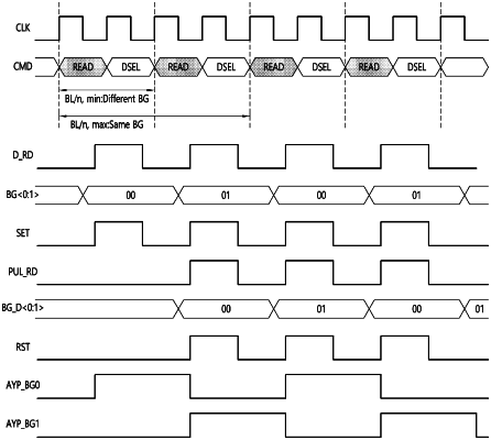
a column path control circuit configured to generate a preliminary column pulse from a command signal irrelevant to a column address signal, to generate a main column pulse in response to an enable time point of the column address signal and an enable time point of the preliminary column pulse, and to enable an access target column line among the plurality of column lines.
|