| CPC G11C 7/1069 (2013.01) [G11C 7/109 (2013.01); G11C 7/1063 (2013.01); G11C 7/1096 (2013.01); G11C 8/06 (2013.01)] | 32 Claims |
|
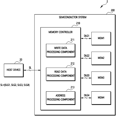
13. A semiconductor system comprising:
a plurality of memory devices; and
a memory controller coupled to the plurality of memory devices respectively through a plurality of device line groups and coupled to a host device through system lines,
wherein the memory controller includes a write data processing component configured to:
receive, from the host device, base device information indicating a base device among the plurality of memory devices,
map, based on the base device information, the plurality of device line groups and a plurality of system line groups, which are divided from the system lines, and
transfer data, which are provided from the host device through the plurality of system line groups, to the plurality of device line groups mapped to the plurality of system line groups, respectively.
|