| CPC G11C 7/1039 (2013.01) [G11C 7/1057 (2013.01); G11C 7/1096 (2013.01); H03K 19/0005 (2013.01); H03K 19/01742 (2013.01)] | 7 Claims |
|
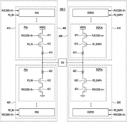
1. A data output buffer comprising:
a first driver configured to drive a data input/output (I/O) pad according to an input signal and allow data drivability to be controlled according to an impedance calibration code; and
a second driver configured to directly receive emphasis signals and the impedance calibration code, perform a de-emphasis operation on the data I/O pad and allow de-emphasis drivability to be controlled according to the impedance calibration code.
|