| CPC G11C 5/063 (2013.01) [G11C 7/1051 (2013.01); G11C 11/4074 (2013.01); G11C 11/4091 (2013.01); H01L 29/7869 (2013.01); H10B 12/30 (2023.02); H10B 12/50 (2023.02)] | 13 Claims |
|
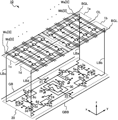
1. A semiconductor device comprising:
a first layer comprising a circuit; and
a second layer over the first layer, the second layer comprising:
a first memory cell comprising a first transistor comprising an oxide semiconductor in a channel formation region; and
a second memory cell comprising a second transistor comprising an oxide semiconductor in a channel formation region,
wherein each of the first transistor and the second transistor comprises a front gate and a back gate,
wherein the back gate of the first transistor is electrically connected to the back gate of the second transistor,
wherein one of a source and a drain of the first transistor is electrically connected to a first electrode of a first capacitor,
wherein one of a source and a drain of the second transistor is electrically connected to a first electrode of a second capacitor,
wherein the other of the source and the drain of the first transistor is electrically connected to a first wiring,
wherein the other of the source and the drain of the second transistor is electrically connected to a second wiring,
wherein the circuit comprises a third transistor, a fourth transistor, a fifth transistor, and a sixth transistor,
wherein a gate of the third transistor is electrically connected to the first wiring,
wherein a gate of the fifth transistor is electrically connected to the second wiring,
wherein one of a source and a drain of the third transistor is electrically connected to one of a source and a drain of the fourth transistor,
wherein one of a source and a drain of the fifth transistor is electrically connected to one of a source and a drain of the sixth transistor, and
wherein a gate of the fourth transistor is electrically connected to a gate of the sixth transistor.
|