| CPC G09G 3/3648 (2013.01) [G09G 3/3225 (2013.01); G09G 2310/06 (2013.01); G09G 2310/08 (2013.01)] | 18 Claims |
|
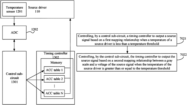
1. A display driving circuit, comprising: a source driver, a temperature detecting circuit, and a timing control circuit, wherein
the temperature detecting circuit is connected to the timing control circuit, and is configured to detect a temperature of the source driver;
the timing control circuit comprises a control sub-circuit and a timing controller; and the timing controller stores a first mapping relationship between gray scales and voltages of a source signal;
the control sub-circuit is connected to the temperature detecting circuit and the timing controller, and the timing controller is further connected to the source driver; and
the control sub-circuit is configured to control the timing controller to output the source signal to the source driver based on the first mapping relationship when the temperature of the source driver is less than a temperature threshold, and to control the timing controller to output the source signal to the source driver based on a second mapping relationship between the gray scales and the voltages of the source signal when the temperature of the source driver is greater than or equal to the temperature threshold;
wherein each voltage of the source signal in the second mapping relationship is determined based on a product of a corresponding voltage of the source signal in the first mapping relationship and a gain coefficient, the gain coefficient being less than 1, and a magnitude of the voltage of the source signal is negatively related to the temperature of the source driver.
|