| CPC G09G 3/3258 (2013.01) [G09G 3/2003 (2013.01); G09G 3/3266 (2013.01); G09G 3/3291 (2013.01); H10K 50/814 (2023.02); H10K 59/124 (2023.02); H10K 59/1213 (2023.02); H10K 59/131 (2023.02); H10K 59/353 (2023.02); G09G 2300/0426 (2013.01); G09G 2300/0443 (2013.01)] | 20 Claims |
|
1. A display substrate, comprising:
a base substrate;
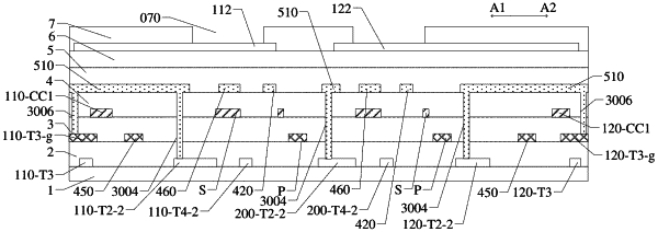
a plurality of sub-pixels on the base substrate, wherein each of the plurality of sub-pixels comprises a light emitting element and a pixel circuit, the light emitting element comprises a first electrode, a light emitting layer and a second electrode which are stacked in sequence, the second electrode is between the light emitting layer and the base substrate, the pixel circuit comprises a driving transistor and a storage capacitor which are between the second electrode of the light emitting element and the base substrate, a gate electrode of the driving transistor is also used as an electrode of the storage capacitor;
wherein the plurality of sub-pixels comprises at least one first color sub-pixel pair and a plurality of sub-pixels of other colors, each first color sub-pixel pair comprises a first pixel block and a second pixel block, a minimum distance between the first pixel block and the second pixel block in each first color sub-pixel pair is not greater than a minimum distance between two sub-pixels of a same color in the plurality of sub-pixels of other colors;
in a same first color sub-pixel pair, an overlapping situation, of orthographic projections of the second electrode of the light emitting element of one first pixel block and the gate electrode of the driving transistor of the one first pixel block on the base substrate, is the same as an overlapping situation, of orthographic projections of the second electrode of the light emitting element of one second pixel block and the gate electrode of the driving transistor of the one second pixel block on the base substrate.
|
|
16. A display substrate, comprising:
a base substrate;
a plurality of sub-pixels on the base substrate, wherein each of the plurality of sub-pixels comprises a light emitting element and a pixel circuit, the light emitting element comprises a first electrode, a light emitting layer and a second electrode which are stacked in sequence, the second electrode is between the light emitting layer and the base substrate, the pixel circuit comprises a first connecting portion, a driving transistor and a threshold compensation transistor which are between the second electrode and the base substrate, the first connecting portion extends in a first direction, a first electrode of the threshold compensation transistor is electrically connected with a first electrode of the driving transistor, and a second electrode of the threshold compensation transistor is electrically connected with a gate electrode of the driving transistor through the first connecting portion,
the plurality of sub-pixels comprises at least one first color sub-pixel pair and a plurality of sub-pixels of other colors, each first color sub-pixel pair comprises a first pixel block and a second pixel block arranged in a second direction, a minimum distance between the first pixel block and the second pixel block in each first color sub-pixel pair is not greater than a minimum distance between two sub-pixels of a same color in the plurality of sub-pixels of other colors, and an included angle between the second direction and the first direction is in a range from 80 degrees to 100 degrees; and
in the first pixel block, an overlapping area between an orthographic projection of the second electrode of the light emitting element on the base substrate and an orthographic projection of the first connecting portion on the base substrate is a first overlapping area; in the second pixel block, an overlapping area between an orthographic projection of the second electrode of the light emitting element on the base substrate and an orthographic projection of the first connecting portion on the base substrate is a second overlapping area; and a ratio of the first overlapping area to the second overlapping area is in a range from 0.8 to 1.2;
in a same first color sub-pixel pair, an overlapping situation, of orthographic projections of the second electrode of the light emitting element of one first pixel block and the gate electrode of the driving transistor of the one first pixel block on the base substrate, is the same as an overlapping situation, of orthographic projections of the second electrode of the light emitting element of one second pixel block and the gate electrode of the driving transistor of the one second pixel block on the base substrate.
|