| CPC G09G 3/32 (2013.01) [G09G 3/2096 (2013.01); G09G 2330/021 (2013.01)] | 11 Claims |
|
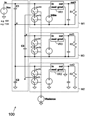
1. A system comprising:
a first, second and third module each comprising an electronic circuit comprising:
an input capacitor connected between a first node and a second node;
a first switch and a second switch connected in series between said first node and said second node, in parallel with said input capacitor, and defining an intermediate node at their interconnection;
a voltage regulator configured for receiving power from said input capacitor and for providing output power at a configurable voltage between an output node and the second node;
wherein the first node of the second module is connected to the second node of the first module,
and wherein the intermediate node of the second module is connected to the second node of the third module;
and wherein the intermediate node of the first module is connected to the first node of the third module;
and wherein the system further comprises a system controller configured for providing a switch control signal of at least 2 MHz to at least the first and the second module, wherein the first and second switch of at least the first and second module are being toggled at a balancing frequency of at least 2 MHz, in such a way that:
during a first moment in time, the first switch of the first and second module are configured to be closed while the second switch of the first and second module are configured to be open,
and during a second moment in time, the first switch of the first and second module are configured to be open while the second switch of the first and second module are configured to be closed,
thereby causing charge distribution between the input capacitor of the first, and second and third module.
|