| CPC G09G 3/20 (2013.01) [H01L 29/1041 (2013.01); G09G 2310/0291 (2013.01)] | 20 Claims |
|
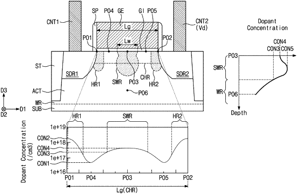
1. A semiconductor device, comprising:
a semiconductor substrate including an active region, the active region defined in a well impurity layer having a first conductivity type;
a gate electrode on the active region; and
a gate insulating layer between the gate electrode and the active region,
wherein the active region comprises
a source region and a drain region, the source region at a first side of the gate electrode, the drain region at a second side of the gate electrode, and the source region and the drain region having a second conductivity type,
a channel region between the source and drain regions, the channel region having the first conductivity type,
a first halo region in contact with the source region and a second halo region in contact with the drain region, the first halo region and the second halo region having the first conductivity type, and
a slit well region between the first and second halo regions, the slit well region having the first conductivity type, wherein a top surface of the slit well region is in contact with a bottom surface of the gate insulating layer.
|