| CPC G06T 7/0006 (2013.01) [G03F 1/36 (2013.01); G06F 18/2148 (2023.01); G06F 18/22 (2023.01); G06T 7/50 (2017.01); G06T 7/60 (2013.01); G06V 10/30 (2022.01); G06V 10/42 (2022.01); G06V 10/88 (2022.01); G06T 2207/10061 (2013.01); G06T 2207/20081 (2013.01); G06T 2207/20084 (2013.01); G06T 2207/30148 (2013.01)] | 20 Claims |
|
1. A method of fabricating a semiconductor device comprising:
generating an optical proximity correction (OPC) model;
generating first layout data;
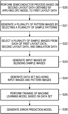
applying the OPC model to the first layout data to generate second layout data;
performing simulation on the second layout data to generate simulation data;
generating a mask based on the second layout data;
performing a semiconductor process using the mask on a substrate;
obtaining a plurality of pattern images by selecting a plurality of sample patterns from the substrate;
selecting a plurality of first sample images corresponding to the plurality of sample patterns, a plurality of second sample images corresponding to the plurality of sample patterns, and a plurality of third sample images corresponding to the plurality of sample patterns, from the first layout data, the second layout data, and the simulation data, respectively;
generating a plurality of input images by blending the plurality of first sample images, the plurality of second sample images, and the plurality of third sample images, each input image being a blended image of: a corresponding one of the plurality of first sample images, a corresponding one of the plurality of second sample images, and a corresponding one of the plurality of third sample images; and
generating an error prediction model for the OPC model by training a machine learning model using a data set including the plurality of input images and the plurality of pattern images.
|