| CPC G06T 7/0004 (2013.01) [G06F 18/214 (2023.01); G06F 18/2431 (2023.01); G06N 3/04 (2013.01); G06N 3/08 (2013.01); G06V 10/764 (2022.01); G06V 10/774 (2022.01); G06V 10/776 (2022.01); G06V 10/7715 (2022.01); G06V 10/82 (2022.01); G06T 2207/20081 (2013.01); G06T 2207/20084 (2013.01); G06T 2207/30148 (2013.01); G06V 2201/06 (2022.01)] | 33 Claims |
|
1. A device, comprising:
image generation circuitry, which, in operation, generates a digital image representation of a wafer defect map (WDM); and
convolutional-neural-network (CNN) circuitry, which, in operation, generates a defect classification associated with the WDM based on:
the digital image representation of the WDM; and
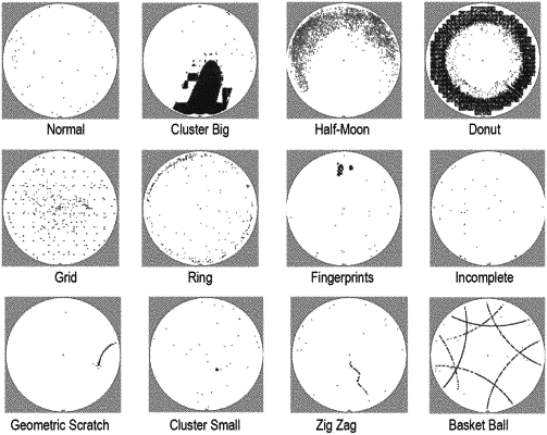
a data-driven model associating WDM images with classes of a defined set of classes of wafer defects and generated using a data set of images, wherein the data set of images includes training images and augmented images generated based on defect pattern orientation types associated with the training images.
|