| CPC G06F 30/398 (2020.01) [G03F 1/36 (2013.01); G03F 7/705 (2013.01); G03F 7/70441 (2013.01); G06F 2119/18 (2020.01); G06F 2119/22 (2020.01)] | 17 Claims |
|
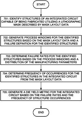
1. A method comprising:
identifying, by a computing system, structures of an integrated circuit capable of being fabricated utilizing a lithographic mask described by mask layout data;
determining, by the computing system, failure rates for the identified structures by:
generating the process windows for the identified structures based, at least in part, on a lithographic response of the mask layout data and a failure definition for the integrated circuit, and
integrating a distribution of manufacturing parameters during fabrication over the generated process windows for the identified structures;
determining, by the computing system, frequency of occurrences for the identified structures in the integrated circuit from the mask layout data; and
generating, by the computing system, a die yield metric for the integrated circuit based, at least in part, on the failure rates for the identified structures and frequency of occurrences for the identified structures in the integrated circuit.
|