| CPC G06F 11/1068 (2013.01) [G11C 11/5642 (2013.01); G11C 11/5671 (2013.01); G11C 16/0483 (2013.01); G11C 16/26 (2013.01)] | 16 Claims |
|
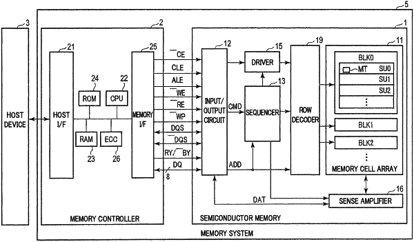
1. A method of controlling a semiconductor memory, the semiconductor memory including a word line and a plurality of memory cells connected to the word line, each of the memory cells being capable of storing n bit data, n being an integer equal to or larger than 2; the method comprising:
storing n pages of data in the memory cells;
reading data of a first page of the n pages as first data using a first voltage;
performing error correction on the first data;
calculating a first shift amount based on a first number and a second number, the first number representing a number of bits each of which has different values in a first manner between the first data and first expected data obtained by the error correction on the first data, the second number representing a number of bits each of which has different values in a second manner between the first data and the first expected data; and
reading data of a second page of the n pages as second data using a second voltage and a second shift amount, the second shift amount being based on the first shift amount.
|