US 11,698,726 B2
Apparatuses and methods for configurable memory array bank architectures
Dean D. Gans, Nampa, ID (US); and Shunichi Saito, Ebina (JP)
Assigned to Micron Technology, Inc., Boise, ID (US)
Filed by MICRON TECHNOLOGY, INC., Boise, ID (US)
Filed on Dec. 20, 2021, as Appl. No. 17/645,101.
Application 17/645,101 is a continuation of application No. 17/033,341, filed on Sep. 25, 2020, granted, now 11,209,981.
Application 17/033,341 is a continuation of application No. 16/452,424, filed on Jun. 25, 2019, granted, now 10,788,985, issued on Sep. 29, 2020.
Application 16/452,424 is a continuation of application No. 16/022,421, filed on Jun. 28, 2018, granted, now 10,372,330, issued on Aug. 6, 2019.
Prior Publication US 2022/0187988 A1, Jun. 16, 2022
Int. Cl. G06F 12/10 (2016.01); G06F 3/06 (2006.01)
CPC G06F 3/0604 (2013.01) [G06F 3/0629 (2013.01); G06F 3/0673 (2013.01); G06F 12/10 (2013.01); G06F 2212/1012 (2013.01)] 18 Claims
OG exemplary drawing
 
1. A method comprising:
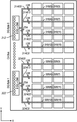
programming a value in a mode register of a memory to select a bank architecture from a plurality of bank architectures, wherein each bank architecture of the plurality of bank architectures comprises a plurality of memory banks of the memory arranged according to the bank architecture selected by the value programmed in the mode register;
mapping addresses to a memory array comprising the plurality of memory banks based, at least in part, on the bank architecture selected; and
switching between a first one and a second one of the plurality of bank architectures during a frequency set point operation.