| CPC G05F 1/56 (2013.01) [G06F 21/755 (2017.08)] | 20 Claims |
|
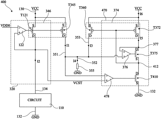
1. A device for powering an electronic circuit, the device comprising:
a first transistor having a drain terminal coupled to a node, a first current flowing at the drain terminal of the first transistor;
a second transistor having a drain terminal coupled to the electronic circuit, a second current flowing at the drain terminal of the second transistor that is an image of the first current, a control terminal of the first transistor coupled to a control terminal of the second transistor;
a third transistor having a drain terminal coupled to the node, a third current flowing at the drain terminal of the third transistor;
a resistive element coupled to the node, a fourth constant current flowing through the resistive element;
a fourth transistor having a control terminal coupled to a control terminal of the third transistor, a fifth current flowing at a drain terminal of the fourth transistor that is an image of the third current; and
a fifth transistor configured to regulate a potential of the node by acting on a control terminal of the fifth transistor electrically in series with the drain terminal of the fourth transistor.
|