| CPC G03F 1/36 (2013.01) [G06F 30/392 (2020.01); G06N 20/00 (2019.01)] | 19 Claims |
|
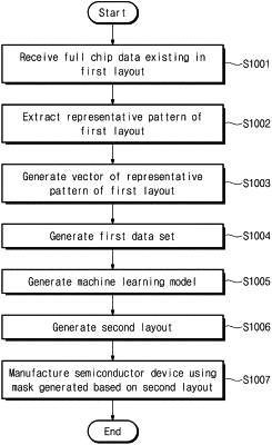
1. A non-transitory computer-readable medium storing codes that, when executed by a processor, cause the processor to perform operations of:
receiving full chip data including specific patterns of a first layout;
extracting a representative pattern of the first layout from the full chip data;
generating a vector of the extracted representative pattern;
generating a first data set based on the generated vector;
generating a machine learning model by performing machine learning with respect to the first data set;
executing an optical proximity correction (OPC) with respect to the specific patterns of the first layout by using the machine learning model;
generating a second layout based on a result of executing the OPC; and
causing to generate a mask for manufacturing a semiconductor device based on the second layout.
|