| CPC G02F 1/153 (2013.01) [G02F 2201/501 (2013.01); G02F 2201/508 (2013.01)] | 16 Claims |
|
1. A method of manufacturing electrochromic devices, the method of manufacturing comprising:
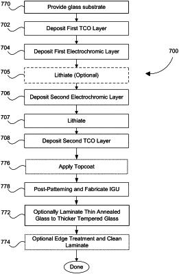
(a) fabricating an electrochromic device comprising an electrochromic stack between a first and a second transparent electrically conductive layer on a glass substrate without pre-patterning in a first facility, wherein pre-patterning comprises determining a location of one or more bus bars to be applied to the first and second transparent electrically conductive layer or cutting the glass substrate into multiple electrochromic lites;
(b) providing a hermetic top coat on the electrochromic device;
(c) after providing the hermetic top coat, shipping the glass substrate to a second facility; and
(d) performing post-processing in the second facility,
wherein (d) comprises performing a process selected from the group consisting of cutting the glass substrate into multiple electrochromic lites, laser patterning of the electrochromic device, and applying one or more bus bars to the electrochromic device, and
wherein the hermetic top coat is applied to the second transparent electrically conductive layer.
|