| CPC G02F 1/1368 (2013.01) [G02F 1/136227 (2013.01); G02F 2201/121 (2013.01); G02F 2201/123 (2013.01)] | 15 Claims |

|
1. A display device comprising:
a first insulating substrate including a round portion of a part of an outer shape of the first insulating substrate;
an inorganic insulating film including a first surface facing the first insulating substrate and a second surface opposite to the first surface;
a first transparent conductive layer on the first surface;
a second transparent conductive layer on the second surface; and
a common voltage metal line, wherein
the first transparent conductive layer includes a plurality of first electrodes arrayed in a matrix in a display portion,
the second transparent conductive layer includes a plurality of second electrodes arrayed in a matrix in the display portion and a third electrode separated from the plurality of second electrodes,
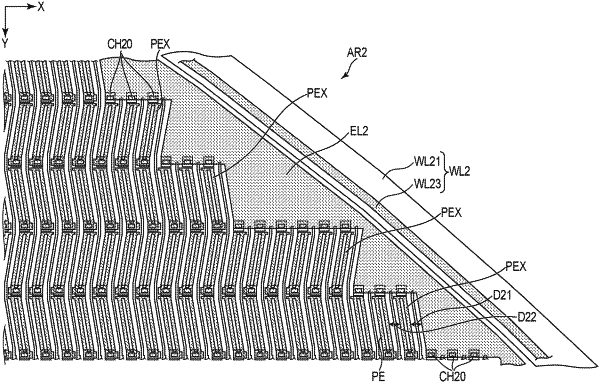
the common voltage metal line is located in a non-display portion outside the display portion and extends along the round portion,
the third electrode spreads over a space between each of the second electrodes and the common voltage metal line in an area close to the round portion, and
an edge of the third electrode, which faces the second electrodes, has a zig-zag shape in the area close to the round portion.
|