| CPC G02F 1/134372 (2021.01) [G02F 1/1323 (2013.01); G02F 1/13338 (2013.01); G02F 1/133345 (2013.01); G02F 1/134336 (2013.01); G02F 1/134345 (2021.01); G02F 1/136286 (2013.01); G06F 3/0412 (2013.01); G06F 3/0446 (2019.05)] | 6 Claims |
|
1. A liquid crystal display device comprising:
a liquid crystal panel; and
a control circuit,
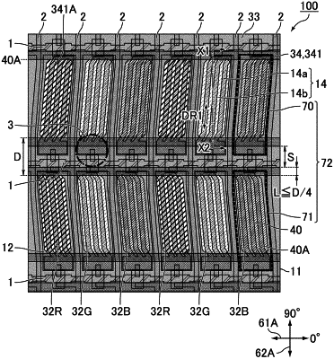
the liquid crystal panel including sub-pixels arranged in a matrix pattern in an in-plane direction and sequentially including an active matrix substrate, a liquid crystal layer containing liquid crystal molecules, and a counter substrate,
the active matrix substrate including a first substrate, a gate line, a first electrode, and a second electrode, the first electrode and the second electrode being stacked with an insulating layer in between,
the counter substrate including a second substrate and a third electrode,
each of the sub-pixels being provided with an optical opening allowing light to pass through the liquid crystal panel,
the third electrode not being superimposed with at least a portion of the optical opening in a plan view and including a linear electrode extending along the gate line,
in a direction perpendicular to an extending direction of the gate line, a distance between the linear electrode and the optical opening being less than D/4 and a width of the linear electrode being D/4 or less, wherein a distance between two optical openings adjacent in the direction perpendicular to the extending direction of the gate line is defined as D,
the control circuit being configured to switch between application of alternating voltage and application of constant voltage to the third electrode.
|