| CPC G02F 1/134336 (2013.01) [G02F 1/1368 (2013.01); G02F 1/13439 (2013.01); G02F 1/133345 (2013.01); G02F 1/134363 (2013.01); G02F 1/136227 (2013.01); G02F 1/136286 (2013.01); H01L 27/1222 (2013.01); H01L 27/1244 (2013.01); H01L 29/78669 (2013.01); H01L 29/78678 (2013.01); G02F 1/133357 (2021.01); G02F 1/134372 (2021.01); G02F 1/136295 (2021.01); G02F 2201/121 (2013.01); G02F 2201/123 (2013.01); G02F 2201/40 (2013.01); G02F 2202/103 (2013.01); G02F 2202/104 (2013.01)] | 18 Claims |
|
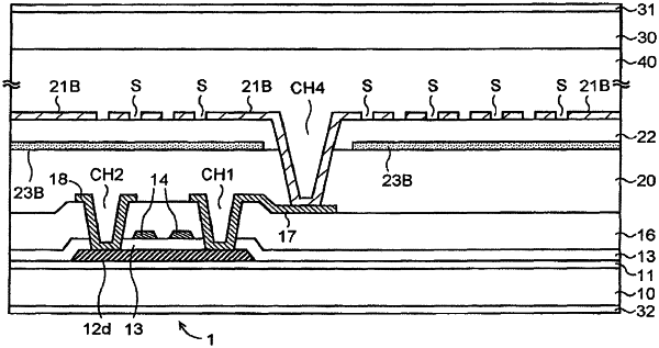
1. A display device comprising:
a first substrate;
a second substrate; and
a liquid crystal layer disposed between the first substrate and the second substrate, the first substrate comprising:
a plurality of pixels arranged in a display portion, each of the pixels including a pixel electrode;
a plurality of thin film transistors, each electrically connected to a corresponding one of the pixel electrodes;
a plurality of signal lines electrically connected to the thin film transistors;
a common electrode opposed to the pixel electrodes, the liquid crystal layer being controlled by an electric field between the pixel electrodes and the common electrode;
a first insulating film interposed between the pixel electrodes and the common electrode;
a second insulating film disposed under the common electrode and the pixel electrodes;
a first common line being disposed along at least one side of the display portion and intersecting the signal lines, in plan view;
a plurality of contact holes each electrically coupling the first common line and the common electrode;
a plurality of gate lines electrically connected to the thin film transistors;
a second common line being disposed along at least another side of the display portion and intersecting the gate lines, in plan view, a plurality of contact holes each electrically coupling the second common line and the common electrode; and
a bridge that is disposed at an intersection of the first common line and one of the signal lines, the bridge being formed in a same layer as the gate lines, wherein the common electrode overlaps the entire area of the display portion,
wherein
the contact holes are arranged in a first direction along the first common line in such a manner that a distance between the contact holes in the first direction is less than a length of each pixel in the first direction, and
the contact holes are arranged in a second direction along the second common line in such a manner that a distance between the contact holes in the second direction is less than a length of each pixel in the second direction.
|