| CPC G02F 1/13338 (2013.01) [H01L 27/1225 (2013.01); H01L 27/1255 (2013.01); H01L 29/24 (2013.01); H01L 29/7869 (2013.01); G02F 1/13454 (2013.01); G06F 3/0412 (2013.01)] | 16 Claims |
|
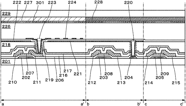
1. A display device having a display portion comprising:
a first substrate;
a second substrate; and
a liquid crystal layer provided between the first substrate and the second substrate,
wherein the display portion includes a sensor unit and a first pixel,
wherein the sensor unit includes a first capacitor comprising a first electrode and a second electrode,
wherein the first electrode comprises a first part of a first conductive film and the second electrode comprises a second conductive film,
wherein the first conductive film faces the second conductive film via the liquid crystal layer,
wherein the first pixel includes a transistor and a first pixel electrode electrically connected to the transistor,
wherein the transistor, the first conductive film, and the first pixel electrode are provided between the first substrate and the liquid crystal layer,
wherein the first conductive film is provided between the transistor and the first pixel electrode,
wherein the first part of the first conductive film does not overlap with the first pixel electrode, and
wherein a second part of the first conductive film has a region overlapped with the first pixel electrode.
|