| CPC G02B 9/12 (2013.01) [G02B 1/002 (2013.01); G02B 3/08 (2013.01); G02B 5/1876 (2013.01); G02B 9/10 (2013.01); G02B 9/14 (2013.01); G02B 13/003 (2013.01); G02B 13/0035 (2013.01); G02B 13/0055 (2013.01); G02B 13/18 (2013.01); G02B 27/0025 (2013.01); H04N 23/55 (2023.01); H05K 999/99 (2013.01); G02B 2207/101 (2013.01)] | 22 Claims |
|
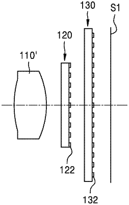
1. An imaging apparatus comprising:
a first optical device configured to transmit light;
a second optical device configured to transmit the light transmitted through the first optical device that is incident on the second optical device; and
a third optical device disposed such that the light transmitted through the second optical device is incident on the third optical device,
wherein at least one of the first optical device, the second optical device, and the third optical device comprises a plurality of nanostructures, and heights of at least two nanostructures of the plurality of nanostructures are different from each other,
wherein the first optical device is a refractive optical lens, and each of the second optical device and the third optical device is a thin lens comprising the plurality of nanostructures, and
wherein the plurality of nanostructures of the second optical device and the plurality of nanostructures of the third optical device are configured to offset a chromatic aberration of the second optical device and a chromatic aberration of the third optical device with each other.
|