| CPC G01T 1/2018 (2013.01) [H01L 27/14623 (2013.01); H01L 27/14629 (2013.01); H01L 27/14663 (2013.01); H01L 27/14685 (2013.01); H01L 27/14689 (2013.01); H01L 27/14692 (2013.01)] | 17 Claims |
|
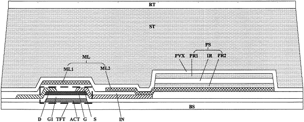
1. A radiation detector having a plurality of pixels, wherein a respective one of the plurality of pixels comprises:
a base substrate;
a thin film transistor on the base substrate;
an insulating layer on a side of the thin film transistor away from the base substrate;
a metallic layer on a side of the insulating layer away from the base substrate;
a photosensor on a side of the insulating layer away from the base substrate;
a passivation layer on a side of the photosensor away from the base substrate;
a scintillation layer on a side of the passivation layer away from the base substrate; and
a reflective layer on a side of the scintillation layer away from the base substrate;
wherein the photosensor comprises a first polarity layer in direct contact with the passivation layer, and a second polarity layer connected to a source electrode of the thin film transistor; and
wherein all sides of the first polarity layer other than a side internal to the photosensor are entirely in direct contact with the passivation layer;
wherein the metallic layer comprises a first part and a second part in a same layer and spaced apart from each other;
the first part is on a side of the insulating layer away from an active layer of the thin film transistor, and configured to shield light from irradiating on the active layer; and
the second part is between the insulating layer and the second polarity layer, is electrically connected to the second polarity layer, and extends through the insulating layer to connect to a source electrode of the thin film transistor.
|