| CPC G01R 31/2884 (2013.01) [H03K 5/24 (2013.01); H03M 1/124 (2013.01)] | 20 Claims |
|
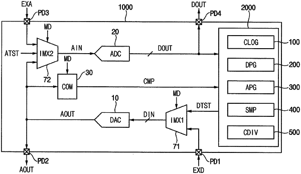
1. A method of testing a semiconductor integrated circuit including an analog-to-digital converter and a digital-to-analog converter, the method comprising:
generating an operational mode control signal;
configuring a first input multiplexer and a second input multiplexer into one of a plurality of different operational test states responsive to the operational mode control signal;
generating an analog test signal having a test pattern using an analog test signal generator or a digital test signal having the test pattern using a digital test signal generator;
generating an analog output signal corresponding to the test pattern by applying, as a digital input signal, the digital test signal having the test pattern to a digital-to-analog converter responsive to generation of the digital test signal and based on the one of the plurality of different operational test states of the first input multiplexer;
generating a digital output signal corresponding to the test pattern by applying, as an analog input signal, the analog test signal having the test pattern or the analog output signal corresponding to the test pattern to an analog-to-digital converter based on the one of the plurality of different operational test states of the second input multiplexer; and
determining a normality of the semiconductor integrated circuit based on the digital output signal corresponding to the test pattern.
|