| CPC G01R 1/07392 (2013.01) [G01R 1/06755 (2013.01); G01R 1/06772 (2013.01); G01R 1/07342 (2013.01); G01R 31/2886 (2013.01)] | 20 Claims |
|
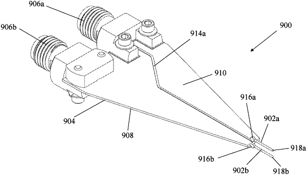
1. A high-frequency testing probe, comprising:
a probe substrate comprising a printed circuit board with a first side and a second side opposite the first side, wherein a thickness of the printed circuit board is smaller than a length and a width of the first side and smaller than a length and a width of the second side;
a plurality of probe connectors having a first probe connector and a second probe connector, the plurality of probe connectors disposed on the printed circuit board and configured to couple the high-frequency testing probe to at least one of a high-frequency vector network analyzer and a high-frequency time domain reflectometer; and
at least two probe tips extending away from the printed circuit board, the at least two probe tips configured to physically contact and test a device through the physical contact, the at least two probe tips comprising:
a first probe tip communicatively coupled to the first probe connector through a first conducting trace disposed on the first side of the printed circuit board, the first probe tip physically coupled to the first conducting trace through a first joint on the first side of the printed circuit board, wherein the first probe tip is configured to rotate about the first joint and extend away from the printed circuit board at an angle within 15 degrees of parallel to the first side; and
a second probe tip communicatively coupled to the second probe connector through a second conducting trace disposed on the second side of the printed circuit board, the second probe tip physically coupled to the second conducting trace through a second joint on the second side of the printed circuit board, wherein the second probe tip is configured to rotate about the second joint and extend away from the printed circuit board at an angle within 15 degrees of parallel to the second side.
|