| CPC G01J 1/0411 (2013.01) [G01J 1/44 (2013.01); G02B 5/1828 (2013.01); G02B 5/1857 (2013.01); H01L 31/02327 (2013.01); H01L 31/1013 (2013.01); G01J 2001/444 (2013.01)] | 18 Claims |
|
1. A light sensor, comprising:
a semiconductor substrate; and
a plurality of pixels, wherein each pixel comprises:
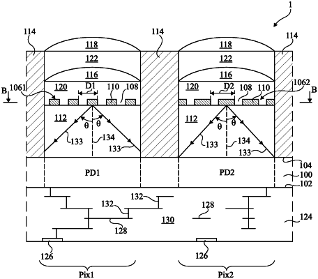
a photoconversion zone extending in the semiconductor substrate between a front face and a back face of the semiconductor substrate;
an optical diffraction grating positioned over the back face of the semiconductor substrate and facing the photoconversion zone of the pixel; and
a wall configured to be absorbent at operating wavelengths of the sensor, said wall positioned to laterally surround the optical diffraction grating of the pixel and extend heightwise from the back face of the semiconductor substrate at least up to a level of the optical diffraction grating of the pixel;
wherein the optical diffraction grating of one pixel of said plurality of pixels and the optical diffraction grating of another pixel of said plurality of pixels have different pitches.
|