| CPC B29C 45/14065 (2013.01) [H05K 1/0203 (2013.01); H05K 5/065 (2013.01); H05K 7/2039 (2013.01); H05K 7/20854 (2013.01); B29L 2031/3425 (2013.01); H05K 2201/066 (2013.01)] | 7 Claims |
|
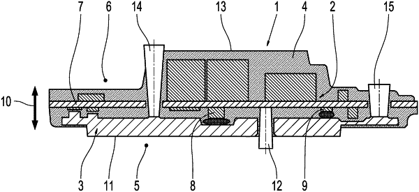
1. A tool for coating an electronic module, the tool comprising:
a first tool part and a second tool part that form a cavity between the first tool part and the second tool part, the cavity being configured to receive a flat circuit board,
wherein the first tool part has a first molding surface section and at least one first supporting section that extends from the first molding surface section towards the second tool part, and
wherein the second tool part has a second molding surface section and at least one second supporting section that extends from the second molding surface section towards the first tool part,
wherein a first supporting plane is formed by the at least one first supporting section and a second supporting plane is formed by the at least one second support section,
wherein the first supporting plane and the second supporting plane are spaced apart and each parallel to a main surface of the circuit board, and
wherein the second supporting section extends through an opening of the circuit board such that the first supporting plane is located between the second molding surface section and the second supporting plane.
|