| CPC H10K 59/60 (2023.02) [H10K 39/32 (2023.02); H10K 59/32 (2023.02); H10K 59/40 (2023.02)] | 20 Claims |
|
1. An electronic device, comprising:
a display stack including,
an exterior structural component;
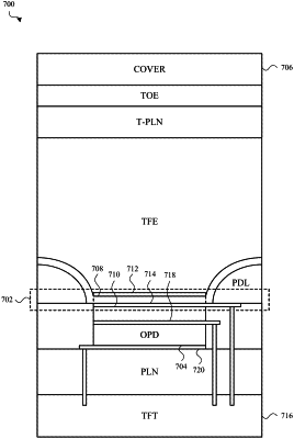
an array of organic light-emitting diodes (OLEDs) disposed below the exterior structural component and including an array of emissive electroluminescent (EL) regions, the array of OLEDs operable to generate an electronic image that is viewable through the exterior structural component;
an array of organic photodetectors (OPDs) disposed below the array of OLEDs; and
at least one reflector positioned between the array of OLEDs and the array of OPDs; wherein,
an emissive EL region of the array of EL regions overlaps an OPD in the array of OPDs;
the emissive EL region emits a first range of electromagnetic radiation wavelengths that passes through the exterior structural component; and
the at least one reflector includes a reflector that reflects at least a first portion of the first range of electromagnetic radiation wavelengths away from the OPD.
|
|
3. An electronic device, comprising:
a display stack including,
an exterior structural component;
an array of organic light-emitting diodes (OLEDs) disposed below the exterior structural component and including an array of emissive electroluminescent (EL) regions, the array of OLEDs operable to generate an electronic image that is viewable through the exterior structural component; and
an array of organic photodetectors (OPDs) disposed below the array of OLEDs, wherein an emissive EL region of the array of EL regions overlaps an OPD in the array of OPDs; wherein,
the array of OPDs has a material construction configured to absorb electromagnetic radiation in at least a first range of electromagnetic radiation wavelengths outside a second range of electromagnetic radiation wavelengths emitted by the array of OLEDs;
a material positioned between the array of OLEDs and the array of OPDs is configured to reflect the second range of electromagnetic radiation wavelengths; and
the first range of electromagnetic radiation wavelengths and the second range of electromagnetic radiation wavelengths are non-overlapping.
|
|
4. An electronic device, comprising:
a display stack including,
an exterior structural component;
an array of organic light-emitting diodes (OLEDs) disposed below the exterior structural component and including an array of emissive electroluminescent (EL) regions, the array of OLEDs operable to generate an electronic image that is viewable through the exterior structural component;
an array of organic photodetectors (OPDs) disposed below the array of OLEDs, wherein an emissive EL region of the array of EL regions overlaps an OPD in the array of OPDs; and
an electrode, positioned between the emissive EL region and the OPD and electrically connected to a surface of the OPD and the emissive EL region.
|
|
15. An electronic device, comprising:
a display stack including,
an exterior structural component;
an array of organic light-emitting diodes (OLEDs) disposed below the exterior structural component and including an array of emissive electroluminescent (EL) regions, the array of OLEDs operable to generate an electronic image that is viewable through the exterior structural component;
an array of organic photodetectors (OPDs) disposed below the array of OLEDs, wherein an emissive EL region of the array of EL regions overlaps an OPD in the array of OPDs; and
a charge generation layer (CGL), positioned between the emissive EL region and a surface of the OPD and configured to charge the emissive EL region and the OPD.
|