| CPC H10K 59/131 (2023.02) [H10K 59/1201 (2023.02)] | 15 Claims |

|
1. A display substrate, comprising: a display region and a non-display region surrounding the display region;
wherein the display substrate further comprises:
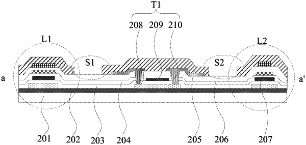
an organic functional layer comprising a first portion located in the display region and a second portion located in the non-display region, wherein the second portion is provided with at least one isolation groove, and is partitioned into at least two separate sub-portions by the at least one isolation groove, and the at least two sub-portions are arranged sequentially along a first direction from the display region to a boundary of the display substrate;
wherein the second portion is provided with a first isolation groove and a second isolation groove, and the first isolation groove is located between the display region and the second isolation groove;
the second portion is partitioned by the first isolation groove and the second isolation groove into a first sub-portion, a second sub-portion and a third sub-portion, and the first sub-portion, the second sub-portion and the third sub-portion are separate from each other, and are sequentially arranged in a spaced manner along the first direction;
wherein the display substrate further comprises:
a circuit structure located in the non-display region, wherein an orthographic projection of the circuit structure onto a base substrate of the display substrate is covered by an orthographic projection of the second sub-portion onto the base substrate;
a first signal line structure located in the non-display region, wherein an orthographic projection of the first signal line structure onto the base substrate is covered by an orthographic projection of the first sub-portion onto the base substrate;
a second signal line structure located in the non-display region, wherein an orthographic projection of the second signal line structure onto the base substrate is covered by an orthographic projection of the third sub-portion onto the base substrate;
wherein along the first direction, both a width of the first sub-portion and a width of the third sub-portion are smaller than a width of the second sub-portion.
|