| CPC H10K 59/131 (2023.02) [H01L 24/05 (2013.01); H01L 24/06 (2013.01); H01L 24/32 (2013.01); H01L 25/18 (2013.01); H01L 2224/05548 (2013.01); H01L 2224/0603 (2013.01); H01L 2224/32145 (2013.01); H01L 2224/32225 (2013.01); H10K 59/88 (2023.02); H10K 77/111 (2023.02); H10K 2102/311 (2023.02)] | 17 Claims |

|
1. A display panel, comprising:
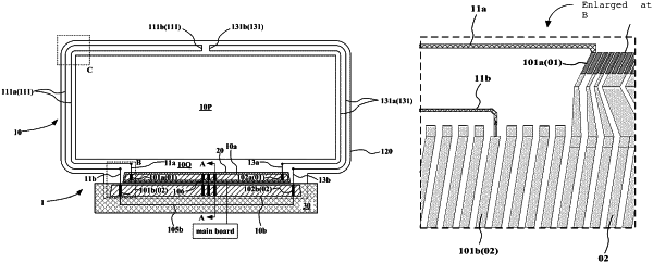
a display substrate comprising a display area and a non-display area surrounding the display area, wherein the display substrate comprises a substrate, as well as a first bonding portion, a second bonding portion, a first connection line and a second connection line, which are located on one side of the substrate and located in the non-display area, wherein:
the first bonding portion comprises a plurality of first pins comprising a first detection pin and a second detection pin;
the second bonding portion is located on one side of the first bonding portion away from the display area and connected to the first bonding portion, the second bonding portion comprises a plurality of second pins comprising a first connection pin and second connection pin;
the first connection line connects the first detection pin to the first connection pin, and comprises a first crack detection line arranged around at least a portion of edges of the display area; and
the second connection line connects the second detection pin to the second connection pin;
an integrated circuit chip bonded to the first bonding portion, and configured to drive the display substrate to display according to a signal of a main board, and to determine whether there is a crack on an edge of the display substrate according to electric signals of the first detection pin and the second detection pin; and
a circuit board bonded to the second bonding portion and configured to transmit a signal of the main board to the integrated circuit chip, wherein the circuit board comprises a connection wire that connects the first connection pin to the second connection pin.
|