| CPC H10K 59/131 (2023.02) | 22 Claims |
|
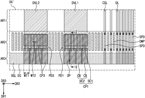
1. A display panel comprising:
a base substrate in which a first area, a second area, and a third area are sequentially defined in a first direction;
pixels disposed on the first area;
signal lines disposed on the base substrate and electrically connected to the pixels;
a power line disposed on the base substrate, wherein the power line supplies a power to the pixels;
signal pads disposed on the second area, arranged in a second direction crossing the first direction, and electrically connected to the signal lines;
power pads disposed on the second area, arranged in the second direction, and electrically connected to the power line; and
a conductive portion comprising a first sub-conductive portion disposed on the second area of the base substrate and overlapping the power pads and a second sub-conductive portion disposed on the third area of the base substrate and spaced apart from the first sub-conductive portion,
wherein the first sub-conductive portion and the second sub-conductive portion are electrically connected to a plurality of the same power pads arranged contiguous to each other in the second direction and the power line, and
wherein an opening is defined in the second sub-conductive portion by a removed portion thereof.
|