| CPC H10K 59/126 (2023.02) [H10K 59/1315 (2023.02); H01L 27/124 (2013.01); H10K 59/1201 (2023.02); H10K 59/1213 (2023.02)] | 16 Claims |
|
1. A display device comprising:
a substrate;
a corrosion prevention layer on the substrate and comprising silicon nitride;
a first conductive layer on the corrosion prevention layer and comprising aluminum or an aluminum alloy;
a first insulating film comprising silicon oxide and silicon nitride on the first conductive layer;
a semiconductor layer on the first insulating film and comprising a channel region of a transistor;
a second insulating film comprising silicon oxide on the semiconductor layer;
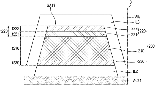
a second conductive layer on the second insulating film and comprising a barrier layer, which comprises titanium, and a main conductive layer, which comprises aluminum or an aluminum alloy;
a capping layer on the main conductive layer and comprising at least one of titanium or a titanium compound;
a third insulating film on the second conductive layer; and
a third conductive layer on the third insulating film,
wherein the semiconductor layer comprises an oxide semiconductor,
wherein the barrier layer is between the semiconductor layer and the main conductive layer and overlaps the channel region of the transistor,
wherein the third conductive layer comprises a source electrode and a drain electrode of the transistor,
wherein the second conductive layer comprises a gate electrode of the transistor,
wherein a thickness of the corrosion prevention layer is in a range of 1000 Å to 2000 Å, and
wherein a thickness of the main conductive layer is in a range of 2500 Å to 4000 Å.
|