| CPC H10K 59/124 (2023.02) [H10K 50/15 (2023.02); H10K 50/16 (2023.02); H10K 50/17 (2023.02); H10K 59/122 (2023.02); H10K 59/353 (2023.02); H10K 59/84 (2023.02); H10K 59/88 (2023.02); H10K 71/00 (2023.02); H10K 59/1201 (2023.02); H10K 59/121 (2023.02); H10K 59/352 (2023.02)] | 4 Claims |
|
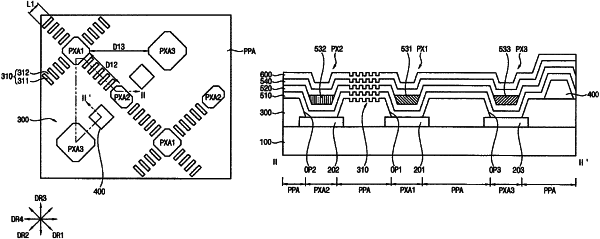
1. A method of manufacturing an OLED device, the method comprising:
forming a first pixel electrode, a second pixel electrode, and a third pixel electrode on a substrate;
forming a pixel defining layer on a face of the substrate, wherein the pixel defining layer comprises a first opening, a second opening, and a third opening respectively partially exposing the first pixel electrode, the second pixel electrode, and the third pixel electrode, wherein the pixel defining layer further comprises an uneven surface and a first flat face, wherein the uneven surface is opposite the first flat face, includes flat faces, and is positioned between the first opening and the second opening, wherein the flat faces are spaced from one another and are parallel to the face of the substrate, wherein the first flat face is positioned between the first pixel electrode and the second pixel electrode and is positioned between the uneven surface and the substrate, and wherein the uneven surface is disposed between the first pixel electrode and the second pixel electrode, and is disposed between the first pixel electrode and the third pixel electrode;
forming a spacer disposed in the pixel defining layer, wherein the spacer is disposed between the second pixel electrode and the third pixel electrode;
forming a first emission layer, a second emission layer, and a third emission layer that respectively correspond to the first opening, the second opening, and the third opening; and
forming a common electrode that overlaps each of the first emission layer, the second emission layer, and the third emission layer.
|