| CPC H10K 59/122 (2023.02) [H10K 50/841 (2023.02)] | 20 Claims |

|
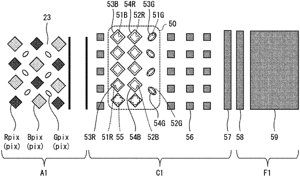
1. A display device comprising a display area and a frame area around the display area, the display area including a stack body including: a thin-film transistor (TFT) layer; a light-emitting element layer including an anode, a functional layer, a cathode, and a pixel bank covering an edge of the anode; and a sealing layer;
the sealing layer including at least one organic film, and a partition wall provided in the frame area, the partition wall being configured to delineate an edge of the at least one organic film;
the display device further comprising, between the display area and the partition wall, a contact area in which the cathode is electrically connected to a metal film made of a same material and in a same layer as the anode; and
an insular test element group (TEG) pattern provided in the contact area, the insular TEG pattern being made of a same material as the functional layer, wherein
the metal film has a first opening at least partially overlapped by the insular TEG pattern when viewed from above with respect to a stacking direction for the stack body.
|