| CPC H10K 59/12 (2023.02) [G09G 3/3233 (2013.01); G09G 2320/0233 (2013.01); H01L 29/1054 (2013.01); H01L 29/66757 (2013.01); H01L 29/7842 (2013.01); H01L 29/78666 (2013.01); H01L 29/78675 (2013.01); H01L 2924/13069 (2013.01); H10K 10/464 (2023.02); H10K 59/1213 (2023.02); H10K 59/35 (2023.02); H10K 77/111 (2023.02); H10K 2102/311 (2023.02)] | 8 Claims |

|
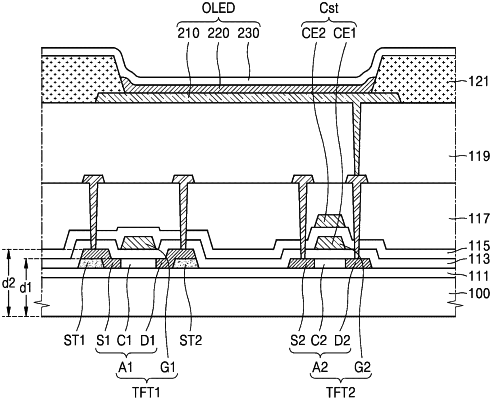
1. A display device comprising:
a first semiconductor layer arranged on a substrate and including a first channel region, a first source region, and a first drain region;
a first stressor arranged between the substrate and the first semiconductor layer and which is overlapped by the first source region in a thickness direction of the first semiconductor layer;
a second stressor arranged between the substrate and the first semiconductor layer and which is overlapped by the first drain region in the thickness direction, the second stressor being spaced apart from the first stressor;
a gate insulating layer arranged on the first semiconductor layer;
a first gate electrode arranged on the gate insulating layer and which overlaps the first semiconductor layer in the thickness direction; and
a second semiconductor layer arranged on a same layer as the first channel region of the first semiconductor layer is disposed on such that an entire lower surface of the second semiconductor layer and an entire lower surface of the first channel region directly contacts the same layer.
|