| CPC H10K 50/858 (2023.02) [G06F 3/0445 (2019.05); H10K 59/12 (2023.02); H10K 59/40 (2023.02)] | 18 Claims |

|
1. A display device comprising:
a substrate;
a light-emitting element on the substrate;
a planarization layer on the light-emitting element;
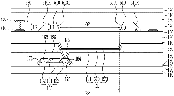
a first refractive index layer outside a light emission region of the light-emitting element on the planarization layer and including a total reflection inclination surface totally reflecting light emitted from the light-emitting element in a front direction and a refraction inclination surface refracting light emitted from the light-emitting element in the front direction;
a second refractive index layer outside the light emission region of the light-emitting element, wherein the second refractive index layer is adjacent to and extends over a portion of the first refractive index layer to be in contact with the refraction inclination surface and having a smaller refractive index than a refractive index of the first refractive index layer; and
a third refractive index layer on the first refractive index layer and the second refractive index layer to be in contact with the total reflection inclination surface and having a larger refractive index than the refractive index of the first refractive index layer.
|