| CPC H10K 50/844 (2023.02) [H10K 50/8426 (2023.02); H10K 59/131 (2023.02); H10K 59/38 (2023.02); H10K 50/131 (2023.02); H10K 50/19 (2023.02); H10K 59/122 (2023.02); H10K 59/124 (2023.02)] | 18 Claims |

|
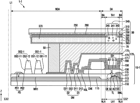
1. A display device comprising:
a first base, on which a display area and a non-display area are defined;
a first support member disposed on the first base and located in the non-display area;
a light emitting element disposed on the first base and located in the display area;
an encapsulation layer disposed on the light emitting element;
a second base disposed on the encapsulation layer;
a color filter disposed between the second base and the encapsulation layer, wherein the color filter overlaps the light emitting element;
a wavelength conversion pattern disposed on the color filter; and
a sealing member disposed between the first base and the second base and located in only the non-display area,
wherein the sealing member is located between the display area and the first support member and overlaps the encapsulation layer, such that the encapsulation layer is disposed above the light emitting element and disposed under the sealing member relative to the first base.
|