| CPC H10K 19/202 (2023.02) [G11C 13/0014 (2013.01); G11C 13/0069 (2013.01); H10K 10/50 (2023.02); H10K 85/221 (2023.02)] | 20 Claims |
|
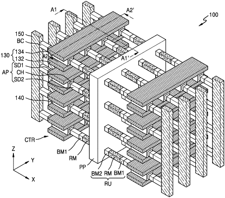
1. A semiconductor memory device comprising:
a plurality of semiconductor patterns extending, above a substrate, in a first horizontal direction and separated from each other in a second horizontal direction and a vertical direction, each semiconductor pattern including
a first source/drain area,
a channel area, and
a second source/drain area arranged in the first horizontal direction;
a plurality of gate insulating layers covering upper surfaces or side surfaces of the channel areas of the plurality of semiconductor patterns;
a plurality of word lines on the upper surfaces or the side surfaces of the channel areas of the plurality of semiconductor patterns; and
a plurality of resistive switch units respectively connected to first sidewalls of the plurality of semiconductor patterns, extending in the first horizontal direction, and separated from each other in the second horizontal direction and the vertical direction, each resistive switch unit including
a first electrode,
a second electrode, and
a resistive switch material layer between the first electrode and the second electrode and including carbon nanotubes.
|